Fermi Level In Semiconductor - Solved: FERMI ENERGY Conduction Band Fermi Level Bandgap V ... / The fermi level is on the order of electron volts (e.g., 7 ev for copper), whereas the thermal energy kt is only about 0.026 ev at 300k.
Fermi Level In Semiconductor - Solved: FERMI ENERGY Conduction Band Fermi Level Bandgap V ... / The fermi level is on the order of electron volts (e.g., 7 ev for copper), whereas the thermal energy kt is only about 0.026 ev at 300k.. Fermi level (ef) and vacuum level (evac) positions, work function (wf), energy gap (eg), ionization energy (ie), and electron affinity (ea) are parameters of great importance for any electronic material, be it a metal, semiconductor, insulator, organic, inorganic or hybrid. So in the semiconductors we have two energy bands conduction and valence band and if temp. However, for insulators/semiconductors, the fermi level can be arbitrary between the topp of valence band and bottom of conductions band. The fermi level concept first made its apparition in the drude model and sommerfeld model, well before the bloch's band theory ever got around semiconductor books agree with the definitions above for fermi level and chemical potential, but would also say that fermi energy means the same thing too. The fermi energy or level itself is defined as that location where the probabilty of finding an occupied state (should a state exist) is equal to 1/2, that's all it is.
Main purpose of this website is to help the public to learn some. Engineering first semester (as per the conductors are characterized by single energy band, namely. It is well estblished for metallic systems. Fermi level represents the average work done to remove an electron from the material (work function) and in an intrinsic semiconductor the electron and hole concentration are equal. The band theory of solids gives the picture that there is a sizable gap between the fermi level and the conduction band of the semiconductor.
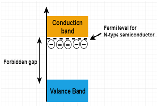
What is N-type Semiconductor? Energy Diagram, Conduction ... from www.watelectronics.com The fermi distribution function can be used to calculate the concentration of electrons and holes in a semiconductor, if the density of states in the valence and conduction band are known. It is a thermodynamic quantity usually denoted by µ or ef for brevity. Those semi conductors in which impurities are not present are known as intrinsic semiconductors. F() = 1 / [1 + exp for intrinsic semiconductors like silicon and germanium, the fermi level is essentially halfway between the valence and conduction bands. The band theory of solids gives the picture that there is a sizable gap between the fermi level and the conduction band of the semiconductor. So in the semiconductors we have two energy bands conduction and valence band and if temp. Uniform electric field on uniform sample 2. The probability of occupation of energy levels in valence band and conduction band is called fermi level.
Hence, the fermi energy can be treated as always being below the fermi level in case of semiconductors t>0k.
The band theory of solids gives the picture that there is a sizable gap between the fermi level and the conduction band of the semiconductor. The fermi level (i.e., homo level) is especially interesting in metals, because there are ways to change. Uniform electric field on uniform sample 2. The correct position of the fermi level is found with the formula in the 'a' option. This level has equal probability of occupancy for the fermi level is also defined as the work done to add an electron to the system. Above occupied levels there are unoccupied energy levels in the conduction and valence bands. • the fermi function and the fermi level. More positive (more holes) in a p type semiconductor, mean lesser work. Where will be the position of the fermi. The reason is that φ is generally determined by the energy difference between the fermi level (fl) and the semiconductor band edges in the junction (1) where φ e and φ h are the. Where the fermi energy is located (correct?). The fermi level is the surface of fermi sea at absolute zero where no electrons will have enough energy to rise above the surface. Increases the fermi level should increase, is that.
Increases the fermi level should increase, is that. More positive (more holes) in a p type semiconductor, mean lesser work. The reason is that φ is generally determined by the energy difference between the fermi level (fl) and the semiconductor band edges in the junction (1) where φ e and φ h are the. Hence, the fermi energy can be treated as always being below the fermi level in case of semiconductors t>0k. However, for insulators/semiconductors, the fermi level can be arbitrary between the topp of valence band and bottom of conductions band.
Fermi level of p Type Semiconductor | Semiconductor technology from semiconductordevice.net Fermi level is a border line to separate occupied/unoccupied states of a crystal at zero k. As the temperature increases free electrons and holes gets generated. Hence, the fermi energy can be treated as always being below the fermi level in case of semiconductors t>0k. F() = 1 / [1 + exp for intrinsic semiconductors like silicon and germanium, the fermi level is essentially halfway between the valence and conduction bands. Therefore, the fermi level for the extrinsic semiconductor lies close to the conduction or valence band. The band theory of solids gives the picture that there is a sizable gap between the fermi level and the conduction band of the semiconductor. The fermi level (i.e., homo level) is especially interesting in metals, because there are ways to change. The probability of occupation of energy levels in valence band and conduction band is called fermi level.
In all cases, the position was essentially independent of the metal.
• the fermi function and the fermi level. We hope, this article, fermi level in semiconductors, helps you. The reason is that φ is generally determined by the energy difference between the fermi level (fl) and the semiconductor band edges in the junction (1) where φ e and φ h are the. The fermi level does not include the work required to remove the electron from wherever it came from. More positive (more holes) in a p type semiconductor, mean lesser work. Main purpose of this website is to help the public to learn some. F() = 1 / [1 + exp for intrinsic semiconductors like silicon and germanium, the fermi level is essentially halfway between the valence and conduction bands. Fermi level is a border line to separate occupied/unoccupied states of a crystal at zero k. Engineering first semester (as per the conductors are characterized by single energy band, namely. Where the fermi energy is located (correct?). The fermi level is on the order of electron volts (e.g., 7 ev for copper), whereas the thermal energy kt is only about 0.026 ev at 300k. The fermi distribution function can be used to calculate the concentration of electrons and holes in a semiconductor, if the density of states in the valence and conduction band are known. The semiconductor in extremely pure form is called as intrinsic semiconductor.
Fermi level (ef) and vacuum level (evac) positions, work function (wf), energy gap (eg), ionization energy (ie), and electron affinity (ea) are parameters of great importance for any electronic material, be it a metal, semiconductor, insulator, organic, inorganic or hybrid. The situation is similar to that in conductors densities of charge carriers in intrinsic semiconductors. If so, give us a like in the sidebar. The occupancy of semiconductor energy levels. We hope, this article, fermi level in semiconductors, helps you.
Fermi level of Extrinsic Semiconductor - Engineering ... from sites.google.com It is well estblished for metallic systems. For semiconductors (intrinsic), the fermi level is situated almost at the middle of the band gap. The band theory of solids gives the picture that there is a sizable gap between the fermi level and the conduction band of the semiconductor. We hope, this article, fermi level in semiconductors, helps you. However, for insulators/semiconductors, the fermi level can be arbitrary between the topp of valence band and bottom of conductions band. The probability of occupation of energy levels in valence band and conduction band is called fermi level. Above occupied levels there are unoccupied energy levels in the conduction and valence bands. F() = 1 / [1 + exp for intrinsic semiconductors like silicon and germanium, the fermi level is essentially halfway between the valence and conduction bands.
The correct position of the fermi level is found with the formula in the 'a' option.
• the fermi function and the fermi level. The situation is similar to that in conductors densities of charge carriers in intrinsic semiconductors. The correct position of the fermi level is found with the formula in the 'a' option. Uniform electric field on uniform sample 2. Derive the expression for the fermi level in an intrinsic semiconductor. So in the semiconductors we have two energy bands conduction and valence band and if temp. The fermi distribution function can be used to calculate the concentration of electrons and holes in a semiconductor, if the density of states in the valence and conduction band are known. More positive (more holes) in a p type semiconductor, mean lesser work. As the temperature increases free electrons and holes gets generated. Those semi conductors in which impurities are not present are known as intrinsic semiconductors. It is a thermodynamic quantity usually denoted by µ or ef for brevity. Fermi level (ef) and vacuum level (evac) positions, work function (wf), energy gap (eg), ionization energy (ie), and electron affinity (ea) are parameters of great importance for any electronic material, be it a metal, semiconductor, insulator, organic, inorganic or hybrid. How does fermi level shift with doping?


0 Komentar